
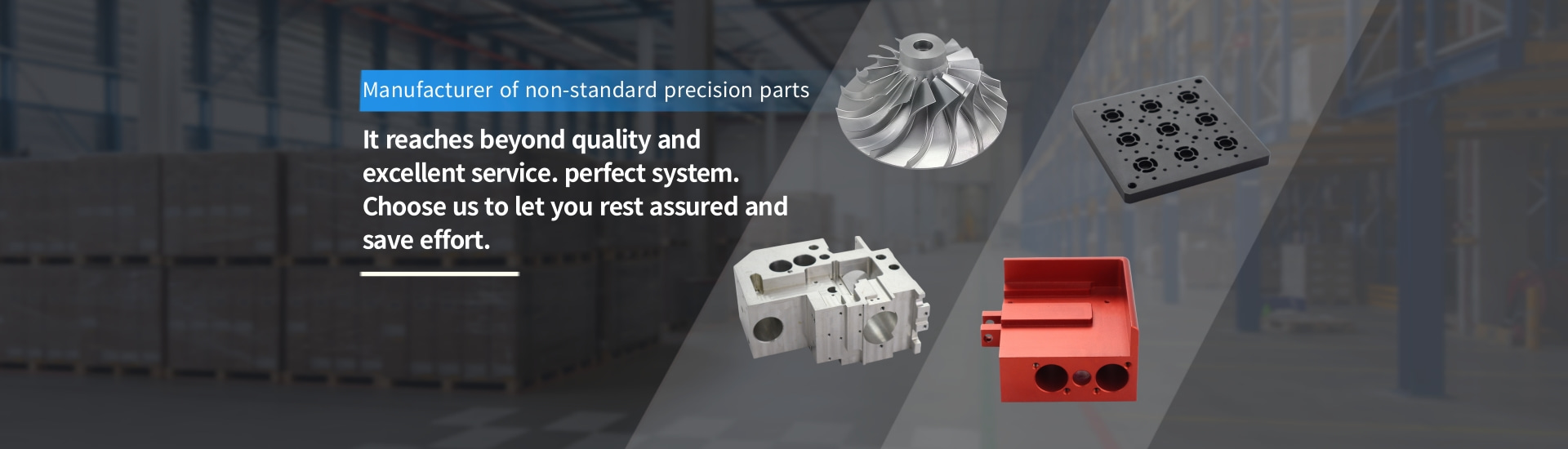
Products Description
Professional black anodizing treatment for optical semiconductor parts
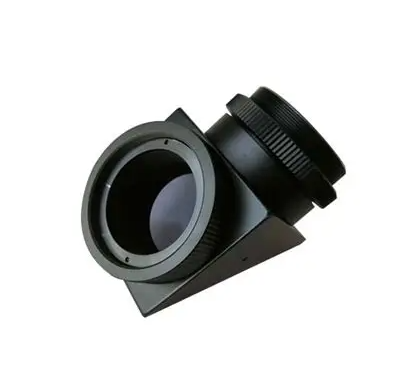
Appearance and StructureShape:
It resembles a composite body, composed of multiple regular or irregular geometric shapes, with obvious right-angle turns, designed to fit specific equipment spaces. Surface Treatment:
The surface of the parts is black and has undergone anodic oxidation treatment, which not only enhances wear resistance and corrosion resistance but may also prevent reflections and static electricity in parts used within semiconductor equipment, ensuring stability in equipment operation.
Interfaces and Mounting Locations:
One side features a larger circular opening, which may be used for optical pathway transmission, lens mounting, or connecting to other components, with structures like threads or slots around the perimeter for fixing; the knob-like structure on the other side is used for adjusting parameters such as optical pathways and focal lengths, allowing for precise micro-adjustments through rotation.
Functional SpeculationOptical Function:
Considering its appearance and structure, it is used in optical inspection and photolithography processes within semiconductor manufacturing, playing a key role in light path bending and focusing. For instance, during the photolithography process, accurately controlling the propagation path of light projects the pattern from the mask onto the wafer accurately.
Precision Positioning:
Semiconductor manufacturing requires extremely high precision; the structures on the parts are used to achieve high-precision positioning and alignment, ensuring that the positional accuracy between various components meets requirements during production, thereby reducing product defects caused by positional deviations.
Application ScenariosSemiconductor Inspection Equipment:
In equipment for wafer inspection and chip appearance inspection, it is used to construct optical systems, assisting inspection devices in obtaining clear and accurate images to assess the quality of semiconductor devices.
Photolithography Machine:
The photolithography machine is the core equipment in semiconductor manufacturing, and this part may serve as a component of its optical pathway system, involved in light bending, focusing, calibration, and other tasks, significantly affecting the precision and quality of photolithography.
| Grand name | QD | Certification | ISO:9001 2015 |
| Processing | turning/milling/lapping/tapping/boring/welding/grinding | Equipment | CMM/Hardness tester/Height gauge/Bore gauge/Microscope |
| LOGO | Accept customization | MOQ | 50000pieces |
Contact Us
Technical Support: +86 150-1532-6863
Email: cassy@xqdmachining.com
Website: https://xqdmachining.com/index.html