Technological innovation and factory practice research of optical semiconductor components
Abstract: This paper focuses on optical semiconductor components in factory production, and conducts research from the aspects of driving factors of technological innovation, manufacturing process optimization, quality control system construction and application in actual production. It aims to explore how to improve the production level of optical semiconductor components through the collaboration of technology and management, and provide theoretical and practical references for the production practices of related factories.
Keywords: optical semiconductor components; technological innovation; manufacturing process; quality control; factory practice.
1.Introduction
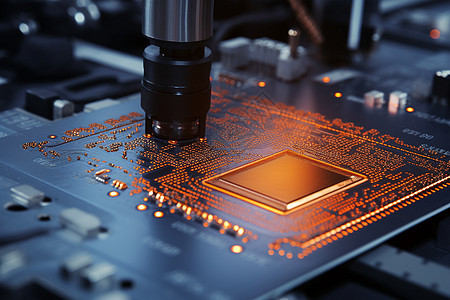
In the modern science and technology landscape, optical semiconductor technology, at the core of the optoelectronics industry, is driving transformation in numerous industries, including communications, healthcare, and consumer electronics. Optical semiconductor components, the fundamental building blocks of optical semiconductor equipment, have a performance and quality that directly impacts the efficiency and stability of the entire optical semiconductor system. Factories, as the primary producers of optical semiconductor components, face growing market demand for high-precision, high-reliability, and diverse components. Therefore, technological innovation and optimized production practices for optical semiconductor components are of vital importance.
2. Driving factors for technological innovation in optical semiconductor components
(一)Driven by market demand
With the rapid development of emerging technologies such as 5G communication, artificial intelligence, and autonomous driving, there are higher demands for the performance of optical semiconductor devices. For example, in the field of 5G communication, high-speed data transmission requires more efficient optical modules, and the core of the optical module—the optical semiconductor components—must possess superior optical performance and higher integration to meet the demands for high bandwidth and low latency transmission. In the consumer electronics market, products such as smartphones and tablets are continuously raising the requirements for pixel count and imaging quality of camera modules, which also drives the optical semiconductor components to develop towards miniaturization and high precision. Changes in market demand force factories to innovate technologically to produce optical semiconductor components that meet the requirements.
(二) Intrinsic requirements of technological development
Optical semiconductor technology itself is in a state of continuous evolution, with the continuous emergence of new materials and principles providing both possibilities and impetus for technological innovation in optical semiconductor components. For example, the development of novel semiconductor materials such as gallium nitride (GaN), with its high electron mobility and other properties, can be used to manufacture high-performance optical semiconductor components, improving their photoelectric conversion efficiency and other performance. Furthermore, advances in micro- and nanofabrication technologies have made it possible to manufacture complex and precise optical semiconductor components on extremely small scales, driving innovation towards miniaturization and high integration.
3. Optimization of Optical Semiconductor Parts Manufacturing Process
(1) Material selection and pretreatment
The performance of optical semiconductor components depends largely on the properties of their materials. Careful selection of suitable semiconductor materials, such as silicon (Si), gallium arsenide (GaAs), and indium phosphide (InP), is crucial for different application scenarios. Indium phosphide, for example, is widely used in the manufacture of lasers, detectors, and other components in the optical communications sector. Its direct bandgap makes it suitable for high-frequency, high-speed optoelectronic devices.
The material pretreatment stage is also crucial. Before use, the materials need to be subjected to rigorous cleaning, polishing, and other treatments to remove surface impurities, scratches, and other defects. For example, using chemical mechanical polishing (CMP) technology can achieve atomic-level flatness on the surface of semiconductor materials, laying the foundation for subsequent precision processing and ensuring consistency in the optical performance of the parts.
(2) Application of precision machining technology
Micro-nanofabrication technology is crucial for the manufacture of optical semiconductor components. Photolithography, a core technology in micro-nanofabrication, enables high-precision structure fabrication by transferring designed patterns onto the surface of semiconductor materials. For example, in the manufacture of components such as optical waveguides, deep ultraviolet lithography can create waveguide structures as small as tens of nanometers in width, precisely controlling the transmission path of light.
Etching technology is also essential. Dry etching (such as reactive ion etching) and wet etching each have their advantages, and the appropriate etching method can be selected based on the component's structural requirements. Dry etching, with its excellent anisotropy and high precision, is suitable for fabricating structures with vertical sidewalls. Wet etching, on the other hand, offers the advantages of low cost and simple processing, making it suitable for fabricating structures requiring relatively low precision. The combined application of these precision machining techniques enables the production of optical semiconductor components with complex three-dimensional structures.
(3) Improvement of surface treatment process
Surface treatment significantly impacts the performance and reliability of optical semiconductor components. For example, black anodizing, such as the components mentioned above, not only imparts a specific appearance and reduces interfering light reflections, but also enhances wear and corrosion resistance. During the treatment process, by optimizing parameters such as electrolyte composition and oxidation voltage, the thickness and properties of the oxide layer can be controlled, ensuring stable performance in complex operating environments.
4. Quality Control System for Optical Semiconductor Parts
(1) Process quality control
The production of optical semiconductor components requires rigorous quality control at every step. Online inspection equipment monitors parameters such as part size, shape, and surface quality in real time during processing. For example, after the photolithography process, an optical microscope or scanning electron microscope (SEM) is used to inspect the line width and alignment accuracy of the photolithographic pattern to ensure accurate pattern transfer. If quality deviations are detected, process parameters are adjusted promptly to avoid defective products and ensure the stability and consistency of the production process.
(2) Finished product inspection and reliability testing
Finished product inspection is a critical step in quality control. High-precision testing instruments, such as laser interferometers and profilometers, are used to comprehensively examine the geometric dimensions and optical properties of parts. Optical semiconductor parts also require optical performance testing, such as measuring transmittance, refractive index, and spectral response, to ensure they meet design requirements.
5. Application Practice of Optical Semiconductor Parts in Factory Production
For example, a factory producing optical communication modules has achieved excellent production results for optical semiconductor laser assemblies, core components of these modules, through the application of these technological innovations and quality control systems. Indium phosphide is used, and rigorous pretreatment ensures high material quality. Advanced lithography and etching techniques are used to create a high-precision laser resonator structure. Combined with an optimized coating process, the lasers achieve high output power and narrow linewidth.
During the production process, in-process quality control monitors the quality of each process in real time, effectively reducing quality fluctuations between processes. Strict finished product inspection and reliability testing ensure that each laser component meets the high standards of the optical communications industry. The application of this component in optical communication modules significantly improves the transmission rate and stability of these modules, meeting the high-speed data transmission requirements of 5G communications. This has been widely recognized in the market, bringing positive economic benefits and market competitiveness to the factory.
6. Conclusion
Optical semiconductor components are the core foundation of optical semiconductor technology, and their technological innovation and production practices are of great significance to the development of the optoelectronics industry. By responding to market demands and technological trends, optimizing manufacturing processes, and establishing a comprehensive quality control system, the factory is able to produce high-precision and high-reliability optical semiconductor components. The successful application of these components in actual production has not only improved the performance of related optical semiconductor equipment but also brought development opportunities to the factory. In the future, with the continuous advancement of science and technology, technological innovation and factory production practices in optical semiconductor components will continue to advance to meet growing market demand and technological challenges.
References:
[1] Zhang Jiexia. Optical Semiconductor Materials and Devices [M]. Beijing: Science Press, 2020.
[2] Li Kaiwen. Application of Micro-nano Processing Technology in Optical Component Manufacturing [J]. Optoelectronic Engineering, 2021, 48 (3): 12-20.
[3] Wang Lu. Optical Thin Film Technology and Its Applications [J]. Advances in Laser and Optoelectronics, 2022, 59 (10): 34-42.